Under Construction
Facilities and Equipment
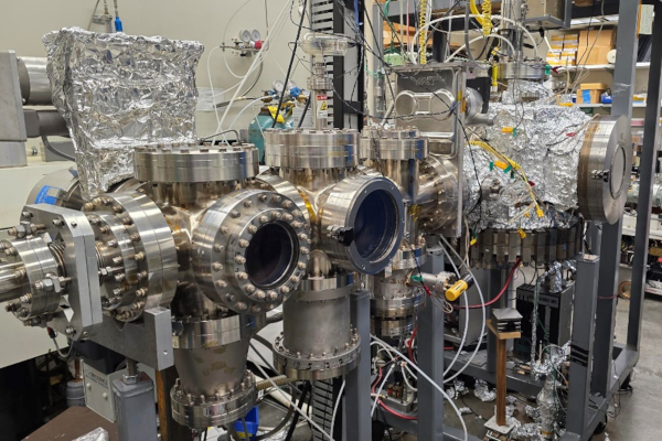
Plasma-Enhanced Chemical Vapor Deposition
Custom-built capacitively coupled plasma-enhanced chemical vapor deposition (PECVD) system connected via in situ transfer to two additional sample prep chambers (configured for RF magnetron sputtering, 2″/3″), equipped with solid-state bubbler system, multiple gas inlets, inverted 8″ showerhead, upper rotating heated (up to 650 °C) substrate holder, and 14″ fast-entry load-lock door. A specialized substrate holder with a range of shadow mask sets allows for the growth of custom batches of multi-layered films/devices on varying substrates.
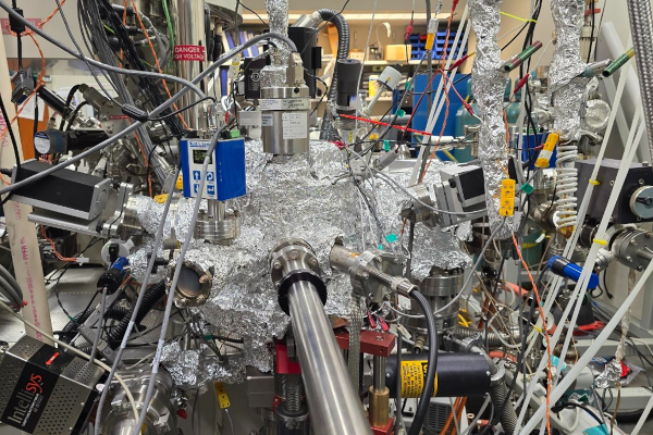
(Plasma-Enhanced) Chemical Vapor Deposition / Atomic Layer Deposition
Custom-built ultra-high-vacuum warm wall chemical vapor deposition (CVD)/atomic layer deposition (ALD) reactor with capacitively coupled plasma capability, resistive substrate heating up to 600 °C, and accommodating multiple solid-state precursor bubblers, ALD valves, and process/plasma gas lines. In-situ thin-film thickness monitoring with a Film Sense FS-1 multi-wavelength ellipsometer, and in-situ sample transfer capability to a custom-built metal evaporation chamber (equipped with Maxtek TM-400 quartz crystal microbalance for monitoring material deposition rate) and X-ray photoelectron spectroscopy (XPS) system.
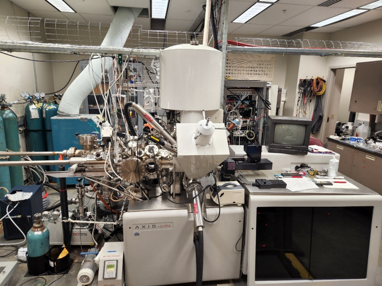
X-Ray Photoelectron Spectroscopy
Kratos Axis Ultra DLD X-ray and ultraviolet photoelectron spectroscopy (XPS/UPS) system with in-situ transfer of samples from two sample preparation chambers (currently equipped with thermal evaporation and chemical vapor deposition/atomic layer deposition capabilities). The system is configured with a dual anode Mg/Al X-ray source, helium UV source, charge neutralizer, and Ar+ sputtering gun for depth profiling and is capable of small spot analysis of 15 μm, surface imaging, as well as angle-resolved XPS. The system enables surface-sensitive quantification of atomic composition and characterization of local chemical bonding, as well as a range of surface and interface electronic structure studies (valence band electronic structure, band lineup…).
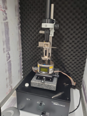
Atomic Force Microscopy
Bruker MultiMode 8 atomic force microscope with PeakForce-TUNA interfaced with the Bruker Nasoscope analysis toolkit for atomic-scale imaging of surfaces. It offers PeakForce ScanAsyst, contact, and tapping mode imaging and can be configured with a variety of different modules for electrical, mechanical, and magnetic property characterization.
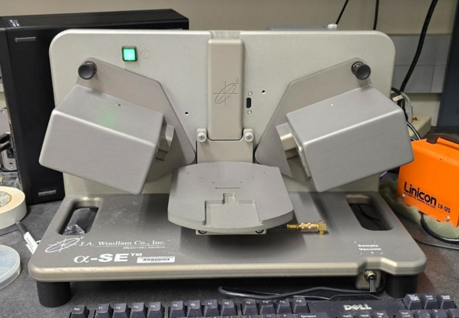
Spectroscopic Ellipsometry
J.A. Woollam Alpha-SE Spectroscopic Ellipsometer for characterization of thin-film thickness from ~1 nm to ~1 um and optical constants, including index of refraction and extinction coefficient.
