Research
We investigate new, unusual, and complex materials for next-generation device technologies such as detectors, optical/electrical switches, and integrated circuit components. We are focused on developing methods and understanding mechanisms of thin-film deposition processes, understanding and optimizing the relationship between atomic/electronic structure and functional properties such as optical, electrical, thermal, and mechanical behavior, and bringing this knowledge together to ultimately design and tune materials to meet the requirements for device integration. Explore our research page to learn more about general areas of interest, and our projects page to see what programs we are working on or have completed.
Materials Design
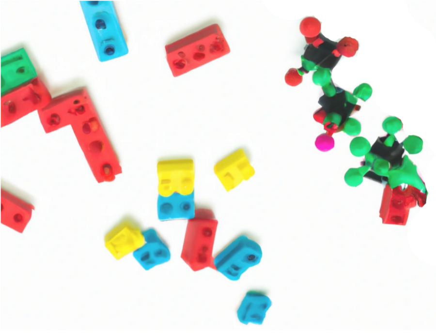
We are interested in understanding the chemical and electronic structure of all sorts of unusual materials and how these can be tuned to optimize functional properties such as electrical or thermal conductivity, mechanical stiffness, or response to a range of electromagnetic fields. We are particularly interested in the challenge posed by disordered solids, which lack a periodic structure and clear global minimum. We are working to bridge the gap between experimental materials data and the use of machine learning to enable the design AND fabrication of real-world materials.
Materials for Devices
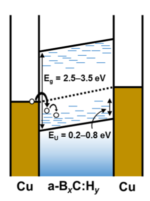
We are interested in the fundamental development of next-generation devices using new materials, especially semi-insulating and wide-band-gap solids. This requires understanding and optimizing the electronic and electrical charge transport properties of a given material alongside other targeted functional properties both within the bulk and at device heterostructure interfaces. We have adapted techniques for measuring charge transport properties in semi-insulating solids, developed theory for extracting charge transport parameters, and investigated interfacial electronic structure including band lineup and charge injection at metal-semiconductor contact interfaces.
Atomic & Molecular Layer Deposition
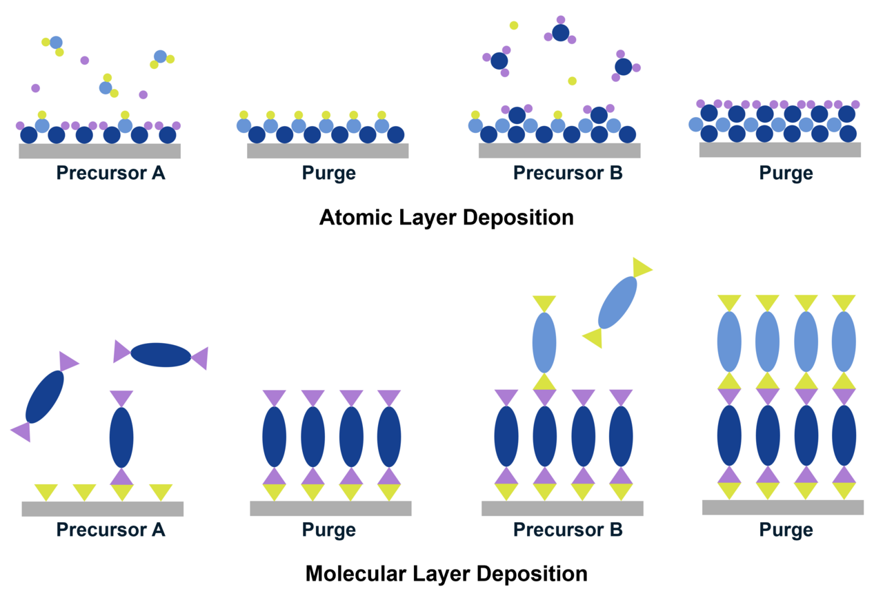
Atomic layer deposition (ALD) is an increasingly popular technique for depositing thin films that enables precise control over material layers at the atomic scale. Through sequential chemical reactions that deposit one layer at a time, films can be deposited that are thin, uniform, and conformal (evenly coating an uneven surface) . Molecular layer deposition (MLD) is likewise based on a layer-by-layer process, but builds up molecular subunits rather than single atoms. We are interested in developing new MLD deposition processes, understanding/optimizing their mechanistic chemistry based on controlled surface science studies, and studying the properties of the resulting functional materials.
Area-Selective Deposition
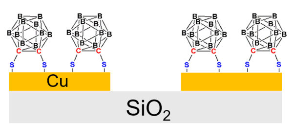
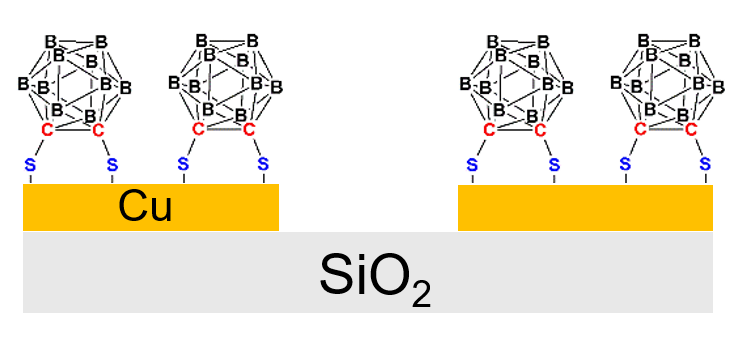
Area-selective deposition (ASD) allows for bottom-up growth on a desired surface while avoiding growth on an adjacent surface. There is substantial interest in expanding the toolbox of available ASD materials and processes to reduce the complexity of and/or increase the fidelity of nanopatterning processes. We are interested in the use of carboranes and other mono- and multi-layer surface chemistries to enable a range of novel selective deposition schemes.
Boron-Rich Solids
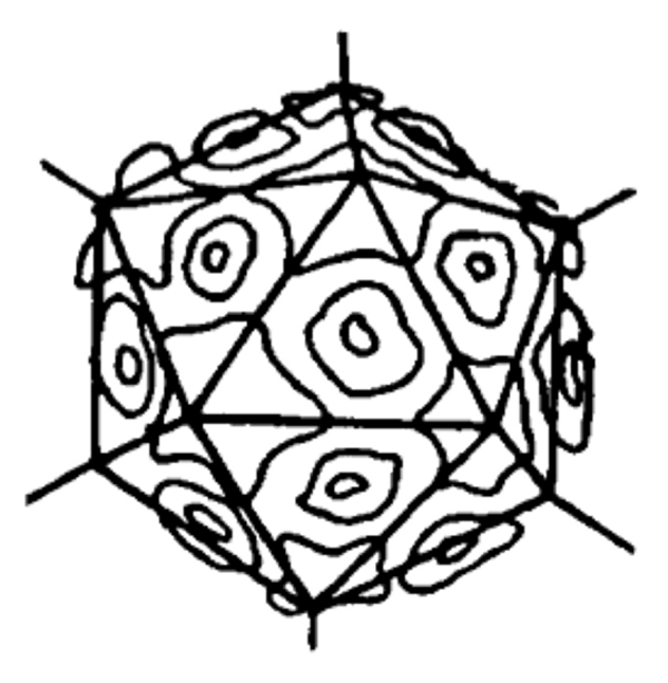
Boron-rich solids are hard, light weight, and possess a range of useful optical and electrical properties. Boron and boron carbide are made up of unique icosahedral structures with unusual (multicenter, delocalized) bonding. Boron nitride, like carbon, can come in a cubic diamond-like structure or a hexagonal graphitic- or graphene-like structure. Amorphous, non-stoichiometric, or doped versions of these materials can quickly pose substantial characterization challenges due to their range of possible electronic and chemical structures. We have investigated boron carbide for neutron detectors, low-k dielectrics, and nanopatterning materials, and are interested in the cutting-edge applications of boron nitride and related material classes.
